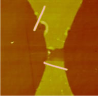
Left: Before manipulation; Right: After manipulation
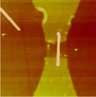
Atomic force microscopes (AFM) can be used to both image and modify samples at molecular or even atomic resolution, in an ambient environment with little to no sample preparation. AFM based nanomanipulation and nanoassembly compares favorably with other techniques such as electron-beam lithography in cost, repeatability, accuracy, and resolution. AFM has thus become a promising tool to prototype nanoscale devices such as single-electron transistors, plasmonic waveguides, to prepare anti-oxidation mask, and to make DNA based circuits. However, fundamental challenges exist in such AFM based nanomanipulation, precluding it from becoming a full-scale manufacturing technology, a) lack of real-time visual feedback since the same tip is used for both manipulation and imaging; b) spatial uncertainties induced by hysteresis, creep and thermal drift that are often larger than the size of nanoscale components; c) unreliable transportation of samples due to varying process conditions such as degrading tip shape, varying temperature and humidity and inherent unstable point-contact between the tip and the sample during manipulation; d) low throughput because of its sequential process nature.
In order to fabricate nanodevices with high throughput, nanomaterials such as nanoparticles and nanowires need to be manipulated towards pre-defined electrodes with high efficiency. Dielectrophoresis (DEP) provides a noninvasive, nondestructive method to effectively align nanowires. Unfortunately, the DEP assisted nanoassembly is very difficult to control and it is almost impossible to guarantee the uniformity of the devices.
The goal of this this research is to develop a nano-robotic system that can enable automated, robust and efficient assembly of nanoscale components such as nanoparticles, carbon nanotubes, nanowires and DNAs into nanodevices by combining AFM based nanomanipulation and the dielectrophoresis assisted nanoassembly. By taking the advantages from both AFM based nanomanipulation and DEP assisted nanoassembly, the nano-robotic system is able to fabricate nanodevice with a high through and a high precision.
Left: Before
manipulation; Right: After manipulation
Papers:
(1) G. Li, L. Liu. Strategic Local Scan for Drift Compensation in AFM Based Nanomanipulation. Under review by IEEE Transactions on Automation Science and Engineering, 2012 (download)
(2) Q. Tao, L. Liu, G. Li. Selective Manipulation of ZnO Nanowires by Controlled Dielectrophoretic Force. Proceedings of the 11th IEEE International Conference on Nanotehcnology. August 15-19, 2011. Portland, Oregon (download).
(3) Q. Tao and G. Li. Simulation Study on Trajectory of Dielectrophoretic Force Controlled Nanowires. Proceedings of the 12th IEEE International Conference on Nanotehcnology. August 20-23, 2012, Birmingham, UK (download)
Sponsor:
 National
Science Foundation Cyber-Physical
Systems Program
National
Science Foundation Cyber-Physical
Systems Program
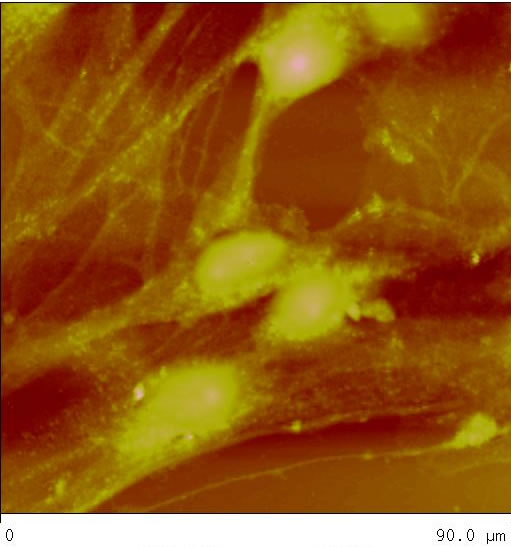
Left:
AFM image of neuron cells; Right: Molelular recognition of angiotensin
II receptors
Papers:
(1) M. Li, L. Liu, N. Xi, Y. Wang, Z. Dong, G. Li. , X. Xiao, W. Zhang. Detecting CD20-Rituximab specific interactions on lymphoma cells using atomic force microscopy. SCIENCE CHINA Life Sciences, 53(10):1189-1195 (2010) (download)
(2) M Li, L. Liu, N. Xi, Y. Wang, Z. Dong, G. Li, X. Xiao, W. Zhang. Detecting CD20-rituximab interaction forces using AFM single-molecule force spectroscopy. Chinese Science Bulletin, 56: 3829-3835, 2011 (cover paper)
The most efficient organic photovoltaic cells (OPVCs) today are made from blending conjugated polymers (donors) and fullerene molecules (acceptors) together to form bulk heterojunctions (BHJs) at nanoscale. The nanoscale morphology of the blend, largely affected by processing conditions, determines the charge generation and transport, and hence dictates the device performance. Despite the importance of morphology, the exact correlations among morphology and performance and processing conditions are still not completely clear due to the lack of in situ characterization tools. Scanning probe microscopes (SPMs) are versatile tools to characterize organic photovoltaic cells in ambient. However, several problems limit the application of SPMs in characterization of organic photovoltaics such as unable to differentiate the donor and acceptor domains in nanoscale and unable to observe the in situ morphological changes during annealing. Therefore, to better understand the physics of organic photovoltaic devices and to find out how the processing conditions affect the nanoscale morphology and hence the device performance, there is a pressing need to develop in situ characterization tools, with which the morphological changes can be monitored in real time with high resolution.
The objective of this research is to find the quantitative correlation among nanoscale morphology and device performance and processing conditions by developing an in situ characterization system that can perform highly sensitive kelvin probe force microscopic study on BHJs to differentiate phase-separated donor and acceptor domains with nanometer scale resolution.
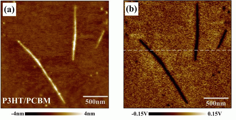
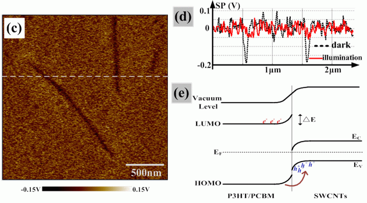
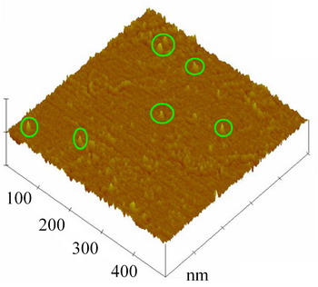
(a) Topography of SWNT bundles on the top of P3HT/PCBM film. (b) SP image in the dark. (c) SP image under illumination. (d) Both SP values of the cross section. (e) heterojunction formed between CNT and P3HT/PCBM
Papers:
(1) L. Liu, W. E. Stanchina, G. Li. Effects of semiconducting and metallic single-walled carbon nano tubes on performance of bulk heterojunction organic solar cells. Appl. Phys. Lett. 94(23):233309, 2009 (download)
(2) L. Liu and G. Li. Electrical characterization of single-walled carbon nanotubes in organic solar cells by Kelvin probe force microscopy. Appl. Phys. Lett. 96(8):083302, 2010 (download)
(3)
G. Li and L. Liu.
Carbon nanotubes for organic solar cells. IEEE Nanotechnology Magazine
5(3):18-24, September, 2011 (download)
Sponsor:
National
Science Foundation Energy
for Sustainability programThe current organic photovoltaic cells with high performance are made of bulk heterojunctions (BHJ) by blending donors and acceptors together. Due in part to the poor balance among the absorption of solar spectrum, the dissociation of excitons, and the collection of charge carriers, the power conversion efficiency of this type of organic photovoltaic cells is still lower than the minimum requirement for commercialization. To obtain best performance for organic BHJ photovoltaic cells, optimization is a necessary process. Optimization by direct experimental studies is neither economical nor effective because of the blindness in the process. Therefore, guidance from theoretical and simulation studies will play a key role in optimizing organic photovoltaic cells. Unfortunately, current theoretical and simulation studies are either fundamentally flawed or lack of experimental supports. The main objective of this research is to solve the unbalance problem in organic BHJ photovoltaic cells by optimizing the device based on nano-structured configuration, valid simulation, and in situ characterization.
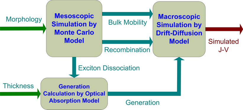
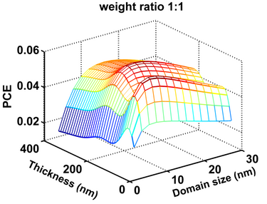
Multiscle simulation takes accout multple aspects at disparate scales and predicates the device performance from the microscopic, mesoscopic, and macroscopic structures.
Papers:
(1)
L. Liu and G.
Li. Investigation
of recombination loss in organic solar cells by simulating
intensity-dependent current–voltage measurements. Solar
Energy Materials and Solar
Cells,
95(9):2557-2563, 2011 (download)
(2) G. Li, L. Liu, F. Wei, S. Xia, and X. Qian. Recent progress in modeling, simulation and optimization of organic solar cells. IEEE J. Photovoltaics, 2(3):320-340, 2012 (download)
(3) F. Wei, L. Liu, Z. Dong, and G. Li. Multiscale modeling and simulation for optimizing polymer bulk heterojunction solar cells. IEEE J. Photovoltaics, 3(1):300-309, 2013. DOI: 10.1109/JPHOTOV.2012.2216507
(4) C. G. Bottenfield, F. Wei, H. J. Park, L. J. Guo, and G. Li. Investigation of printing-based graded bulk heterojunction organic solar cells. Energy Technology, 3(4):414-422, 2015 (DOI: 10.1002/ente.201402152)
(5) M. Jiang, F. Lan, B. Zhao, Q. Tao, J. Wu, D. Gao, and G. Li, Observation of lower defect density in CH3NH3Pb(I,Cl)3 solar cells by admittance spectroscopy, Appl. Phys. Lett. 108, 243501, 2016 (DOI: 10.1063/1.4953834)
Sponsor:
 National
Science Foundation Energy
for Sustainability program
National
Science Foundation Energy
for Sustainability program